
Thermal simulation is an important part of developing power products and providing guidelines for product materials.Optimizing the module form factor is a development trend in terminal equipment design, which brings about the problem of switching from metal heat sinks to PCB copper layer thermal management. Some of today’s modules use lower switching frequencies for switch-mode power supplies and large passive components. Linear regulators are less efficient for voltage translation and quiescent currents that drive internal circuits.
As device designs become increasingly feature-rich, performance-enhancing, and device designs become more compact, thermal simulation at the IC and system levels becomes critical.
Some applications operate at ambient temperatures of 70 to 125C, and some die-size automotive applications can reach temperatures as high as 140C, where uninterrupted system operation is important. Accurate transient and static worst-case thermal analysis for both types of applications is becoming increasingly important when optimizing electronic designs.

Thermal management
The challenge of thermal management is to reduce package size while achieving higher thermal performance, higher operating ambient temperature, and lower budget for copper thermal layers. High packaging efficiency will result in a high concentration of heat-generating components, resulting in extremely high heat fluxes at the IC and package levels.
Factors to consider in the system include some other printed circuit board power devices that may affect the analysis device temperature, system space and airflow design/limitations. There are three layers to consider in thermal management: package, board, and system.
Typical heat transfer paths in an IC package
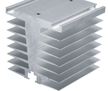
Low cost, small form factor, module integration, and package reliability are a few aspects to consider when choosing a package. As cost becomes a key consideration, leadframe-based thermally enhanced packages are gaining popularity. This package includes embedded heat sink or exposed pad and heat spreader type packages designed to improve thermal performance. In some surface mount packages, special lead frames have several leads fused to each side of the package to act as heat spreaders. This approach provides a better heat dissipation path for heat transfer from the die pad.
IC and Package Thermal Simulation
Thermal analysis requires detailed and accurate silicon die product models and enclosure thermal properties. Semiconductor suppliers provide silicon IC thermal mechanical properties and packaging, while equipment manufacturers provide information on module materials. Product users provide usage environment information.
This analysis helps IC designers optimize power FET dimensions for worst-case power dissipation in transient and quiescent modes of operation. In many power electronics ICs, the power FETs take up a significant portion of the die area. Thermal analysis helps designers optimize their designs.The package chosen typically exposes some of the metal to provide a low thermal impedance path from the silicon die to the heat sink. The key parameters required by the model are as follows:
Silicon die size aspect ratio and die thickness.
Power device area and location, and any auxiliary driver circuits that generate heat.
Power structure thickness (dispersion within the silicon chip).
The die connection area and thickness where the silicon die is connected to exposed metal pads or metal bumps. May include die attach material air gap percentage.
The area and thickness of the exposed metal pad or metal bump connection.
Package size using molding material and connection leads.
The thermal conductivity properties for each material used in the model are required. This data input also includes temperature-dependent changes in all heat transfer properties including:
Silicon chip thermal conductivity
Thermal conductivity of die attach, molding material
Thermal conductivity at the connection of metal pads or metal bumps.
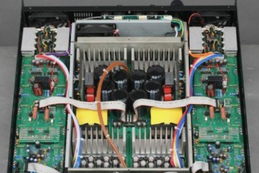
Package product and PCB interaction
A crucial parameter for thermal simulation is to determine the thermal resistance from the pad to the heat sink material, which can be determined in the following ways:
Multilayer FR4 boards (four and six-layer boards are common)
single-ended circuit board
Top and bottom boards
Thermal and thermal resistance paths vary by implementation:
Connect to thermal pads on the internal heat sink panel or thermal vias at bump connections. Use solder to connect exposed thermal pads or bump connections to the top layer of the PCB.
An opening in the PCB below an exposed thermal pad or bump connection that can be connected to a protruding heat sink base that connects to the module’s metal enclosure.
Use metal screws to attach the heat sink to the heat sink on the top or bottom copper layer of the PCB of the metal case. Use solder to connect the exposed thermal pad or bump connection to the top layer of the PCB.
Also, the weight or thickness of the copper plating used on each layer of the PCB is critical. For thermal resistance analysis, layers connected to exposed pad or bump connections are directly affected by this parameter. Generally speaking, this is the top, heat sink, and bottom layers in a multilayer printed circuit board.
In most applications, it can be a two ounce copper (2 ounce copper = 2.8 mils or 71 µm) outer layer and a 1 ounce copper (1 ounce copper = 1.4 mils or 35 µm) inner layer, or All are 1 oz copper cladding. In consumer electronics applications, some even use 0.5 oz copper (0.5 oz copper = 0.7 mils or 18 µm) layers.
Model data
Simulating the die temperature requires an IC floorplan that includes all the power FETs on the die and their actual locations to comply with package soldering guidelines.
The size and aspect ratio of each FET is important for thermal distribution. Another important factor to consider is whether the FETs are powered up simultaneously or sequentially. Model accuracy depends on the physical data and material properties used.
Static or average power analysis of the model requires a short computation time and convergence occurs once the highest temperature is recorded.
Transient analysis requires power versus time data. We recorded the data using a better resolution step than the switching power supply case to accurately capture the peak temperature rise during fast power pulses. This analysis is typically time consuming and requires more data input than static power simulations.
This model simulates epoxy voids in the die attach area, or plating voids in a PCB heatsink. In both cases, epoxy/plating voids can affect the thermal resistance of the package
Definition of heat dissipation
Θja—The die junction representing the surrounding thermal resistance, typically used for thermal package performance comparisons.
Θjc—The die junction representing the thermal resistance at the top of the case.
Θjp—The die junction representing the thermal resistance of the exposed thermal pad, often a good reference for predicting die junction temperature.
Θjb—represents the die junction of the board under a lead thermal resistance path.
Implementation of PCB and Module Housing

The data indicates that some modifications are required to lower the FET maximum temperature on the die near the top layer to prevent hot spots from exceeding the 150C T-junction (see Figure 3). The system user can choose to control the power distribution under this specific sequence, thereby reducing the power temperature on the die.
Thermal simulation is an important part of developing power products. In addition, it guides you through the setting of thermal resistance parameters, from the FET junction of the silicon chip to the implementation of various materials in the product. Once the different thermal resistance paths are understood, many systems can be optimized for all applications.
This data can also be used to determine the criteria for the correlation between the derating factor and the increase in ambient operating temperature. These results can be used to help product development teams develop their designs.