For electronic equipment, the device will fail due to overheating, and its reliable performance will be reduced. Therefore, it is very important to have a good heat dissipation treatment of the circuit board.
In thermal design, PCB is the most important heat source bearing, and its heat sources mainly include three aspects:
(1) Heat generation of electronic components
(2) The heat generated by the PCB itself
(3) Heat from other parts
Among the three heat sources, components generate the largest amount of heat, which is the main heat source, followed by the heat generated by the PCB board. The external heat input depends on the overall thermal design of the system.
In the actual PCB design, the heat dissipation issues that engineers need to consider include the selection of the board, the selection of components, and the layout of components. Next, Banermei will focus on sharing with you some of the heat dissipation treatment in the PCB layout design process.
Heat dissipation in PCB layout design
Layout is an important part of the entire PCB heat dissipation design and plays a pivotal role in PCB heat dissipation. As a designer, you need to consider the following aspects when doing PCB layout:
(1) Consider the centralized design and installation of components with high heat generation and large radiation on another PCB board, so as to conduct separate centralized ventilation and cooling to avoid mutual interference with the motherboard;
(2) The heat capacity of the PCB surface is evenly distributed. Do not place high-power consumption components in a concentrated manner. If it is unavoidable, put short components in the upstream of the airflow, and ensure that sufficient cooling air flows through the heat-concentrated area;
(3) Make the heat transfer path as short as possible;
(4) Make the heat transfer cross section as large as possible;
(5) The layout of components should take into account the influence of heat radiation on surrounding parts. Heat-sensitive parts and components (including semiconductor devices) should be kept away from heat sources or isolated;
(6) Pay attention to the direction of forced ventilation and natural ventilation;
(7) The additional sub-boards and device air ducts are in the same direction as the ventilation;
(8) Make the intake and exhaust as far as possible;
(9) The heating device should be placed above the product as much as possible, and should be placed on the airflow channel when conditions permit;
(10) Components with high heat or high current should not be placed on the corners and surrounding edges of the PCB board, install heat sinks as much as possible, and keep them away from other components, and ensure that the heat dissipation channels are unobstructed.
Are there other solutions to provide the thermal performance of the PCB?
Add heat sink copper foil and copper foil for large area power supplies. As can be seen from the above figure, the larger the area where the copper is connected, the lower the junction temperature.
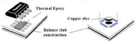
The heat dissipation hole can effectively reduce the junction temperature of the device and improve the temperature uniformity in the thickness direction. The board can adopt other heat dissipation methods on the back of the PCB.
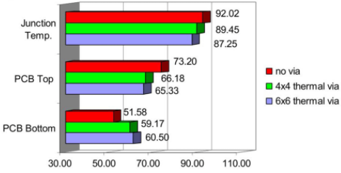
Through simulation, it was found that thermal vias for a device with a thermal power dissipation of 2.5W, a 1mm pitch, and a 6×6 center design can reduce the junction temperature by about 4.8°C compared to non-thermal vias, with a thermal via between the top and bottom of the PCB. temperature difference. from the initial 21°C down to 5°C. After replacing the thermal via array with a 4×4, the junction temperature of the device was 2.2°C higher than that of the 6×6, which is noteworthy.
Exposed copper on the back of the IC reduces the thermal resistance between copper and air.
PCB layout
a. Thermal devices are placed in cold air areas.
b. The temperature sensing device is in the hottest position.
c. Devices on the same printed circuit board should be arranged according to their heat generation and heat dissipation as much as possible. Devices with low heat generation or poor heat resistance (such as small signal transistors, small integrated circuits, electrolytic capacitors, etc.) should be placed. The uppermost stream (at the inlet) of the cooling airflow, devices that generate a lot of heat or heat (such as power transistors, LSIs, etc.) are placed furthest downstream of the cooling. airflow.
d. In the horizontal direction, the high-power devices are placed as close as possible to the edge of the printed circuit board to shorten the heat transfer path; in the vertical direction, the high-power devices are placed as close to the top of the printed circuit board as possible to reduce the heat transfer of other devices while the device is operating temperature. influences.
That is, the heat dissipation of the printed circuit board in the device mainly depends on the airflow, so the airflow path should be studied during the design process, and the device or the printed circuit board should be properly configured. When air flows, it tends to flow where there is low resistance. Therefore, when configuring devices on a printed circuit board, avoid leaving large air spaces in certain areas. The same should be noted when configuring multiple printed circuit boards throughout the machine.
f. Temperature-sensitive equipment should be placed in the lowest temperature area (such as the bottom of the equipment). Do not place it directly over the heating unit. The multiple devices are preferably staggered in a horizontal plane.
g. Place the devices with the highest power consumption and heat generation near the best location for cooling. Do not place higher temperature devices on the corners and perimeter edges of the printed circuit board unless a heat sink is placed near it. When designing power resistors, choose larger devices as much as possible, and have enough room for heat dissipation when adjusting the layout of the printed circuit board.
Conclusion
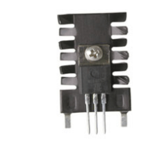
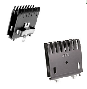
Reminder: It is also a good way to dissipate heat by adding a heat sink to the device. Under normal circumstances, the power of PCB components is relatively small, which is suitable for stamping sheet metal process. This is because the cost of sheet metal heat sinks is low and suitable for mass production. The mold is formed at one time. Moreover, under the conditions of the development of the chip industry, many Standard PCB heat sinks have suitable molds.
Such as Primary Device Types, TO-220, TO-247, TO-126, SOT-32, TO-92, TO-3, TO-5, TO-220, TO-126, SOT-32, so these types of chips Can use stamping heat sink or profile heat sink to dissipate heat. YTthermal engineers have rich experience in the design and selection of PCB heat sinks, especially stamped heat sinks and profile heat sinks, and can customize and design desired products for customers.